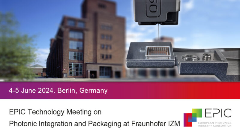
4-5 June 2024
EPIC Technology Meeting on Photonic Integration and Packaging at Fraunhofer IZM
Berlin, Germany
Hosted by

EPIC Meeting on Integrated Photonics at Fraunhofer IZM, a groundbreaking event that brings together industry leaders, experts in photonics, and end-users from around the globe in the dynamic realm of integrated photonics. Hosted by the prestigious Fraunhofer Institute for Reliability and Microintegration (IZM), this meeting aims to foster collaborative discussions and explore the frontiers of integrated photonics technology and scalable packaging of photonic chips. As the demand for faster, smaller, and more efficient electronic devices continues to surge, integrated photonics has emerged as a transformative technology. It offers a myriad of opportunities to revolutionize various sectors, including telecommunications, data centers, healthcare, and sensing applications. Fraunhofer IZM, renowned for its pioneering research in microsystems and packaging technology, is at the forefront of advancing integrated photonics, enabling innovative solutions with unparalleled performance and reliability. The EPIC Meeting serves as a nexus where industry pioneers, entrepreneurs, investors, researchers, and decision-makers can converge to exchange knowledge, share experiences, and collaborate on the future prospects of integrated photonics. With an emphasis on scalable packaging of photonic chips, participants will delve into cutting-edge advancements in chip-scale integration, heterogeneous integration, advanced packaging techniques, and novel manufacturing processes.
Agenda
Accommodation
Company Visits on 3rd June
Speakers
Group Manager
at Fraunhofer IZM

Senior Industrialisation Engineer
at PhotonFirst
Head of Research Unit Electronic Sensors (ELS)
at Silicon Austria Labs
Team Leader
at TESAT

Director Research & Development
at ficonTEC
CEO & Co-Founder
at HETEROMERGE
CCO
at Ligentec
Co-Founder and CTO
at ICON Photonics
CEO
at Nanoscribe
Senior Project Manager
at Fraunhofer HHI
Product Marketing Manager Photonics
at X-FAB
Co-Founder
at Vanguard Automation

Engineering Manager
at Etteplan
Business Development Manager
at EV Group
Chief Operations Officer
at Heidelberg Instruments

Daniel Lieske
Senior Expert Advanced Packaging
at AEMtec

CEO
at AIXEMTEC
Dr. Hektor Meier obtained his PhD from the Swiss Federal Institute of Technology (ETH) in 2011. Shortly after he became a member of the product development team of Enablence Switzerland and later Albis Optoelectronics. He was responsible for the development of ultra high speed InGaAs PIN and avalanche photodiodes. Since 2016 he acts as Head of Product Development at Albis and is in charge of the technology development and expansion of the product portfolio.
Head of Product Development
at Albis Optoelectronics
Senior Analyst
at Yole Group
Research Scientist
at VTT
Manager of the Electro-Optics Group
at NVIDIA
Chief Commercial Officer
at PHIX
Automation Manager
at VLC Photonics
Founder / CEO
at Photonics Foundry
Application Engineer
at EXFO
Attendees
- Andreas Pichler , Regional Sales Manager Europe at EV Group (EVG)
- David de Felipe Mesquida , Senior Project Manager at Fraunhofer HHI
- Elvis Wan , Senior Industrialisation Engineer at PhotonFirst
- Hanano Scheife , Team Leader at TESAT
- Henning Schröder , Group Manager at Fraunhofer IZM
- Ivan-Lazar Bundalo , CTO at InSpek SaS
- Jae-Wung Lee , Reseach Scientist at VTT
- Jan-Jurien de Rijck , Business Development at PhotonFirst Technologies
- Jean-Luc Polleux , Co-Founder and CTO at ICON Photonics
- Jean-Yves Bécel , Export Account Manager at ISP System
- Jeroen Duis , Chief Commercial Officer at PHIX
- Johana Bernasconi , Lead Engineer at Enlightra
- Joni Mellin , Product Marketing Manager Photonics at X-FAB
- Laura Gemini , Deputy Head Laser Processing Dpt. at ALPhANOV
- Martin Hermatschweiler , CEO & Co-Founder at Nanoscribe
- Michael Geiselmann , CCO at Ligentec
- Moritz Seyfried , Director Research & Development at ficonTEC
- Niels Jansen , Manager Engineering at Etteplan
- Philipp Dietrich , Co-Founder at Vanguard Automation
- Pooya Saketi , CEO/Founding Director at Precisement
- Robert Kirchner , CEO & Co-Founder at HETEROMERGE
- Rudolf Heer , Head of Research Unit Electronic Sensors (ELS) at Silicon Austria Labs
- Sebastian Haag , CEO at AIXEMTEC
- Thomas Achleitner , Business Development Manager at EV Group (EVG)
- Tomas Van Stappen , Policy Advisor at Provincie Noord-Brabant
More attendees will be announced soon.
Sponsors
Gold
Bronze


Supported By
Useful resources
Technology Manager
Technology scope and agenda

Ivan Nikitski, PhD
Technology Manager for Quantum and Integrated Photonics
Programme Manager
Coordination

Event Manager
Logistics, venue, accommodation, and transportation
Media Partner/s
Related
Market Reports
Market Reports
2023
Related
Upcoming Events
Upcoming Events
OnLine
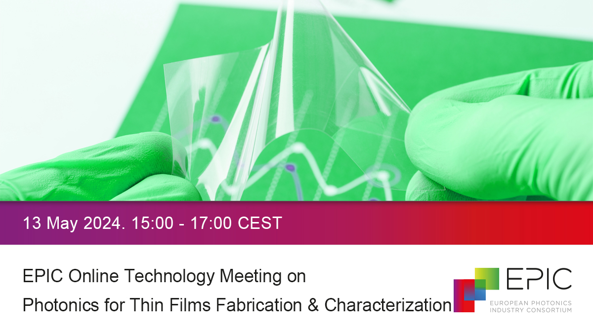
13 May 2024.
Online Event
OnSite
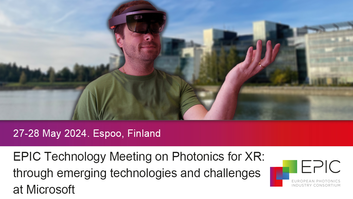
27-28 May 2024.
Espoo, Finland
OnLine

3 June 2024.
Online Event

OnLine

12 June 2024.
Online Event
OnSite
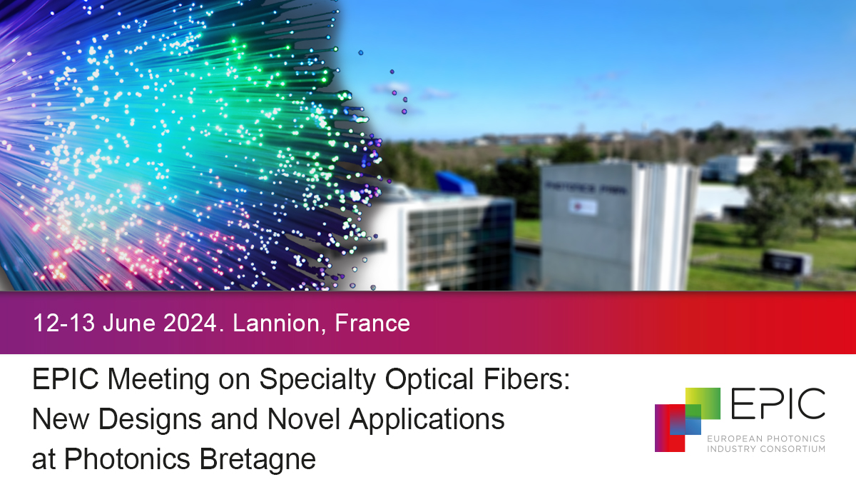
12-13 June 2024.
Lannion, France
Related
Past Events
OnSite
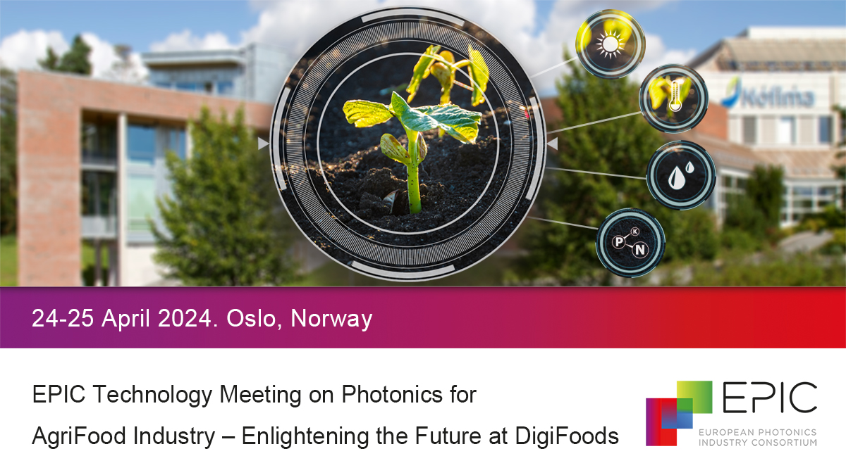
24-25 April 2024.
Oslo, Norway
Registration Closed
OnLine
22 April 2024.
Online Event
Registration Closed